Heavy fermion metals typically contain 4f or 5f elements (e.g. Ce, Yb or U) and hence, local magnetic moments. In these materials, the ground state sensitively depends on the balance between two competing interactions, which are both determined by the hybridization strength J between the spins of the localized 4f or 5f shells and those of the conduction electrons (see Doniach's phase diagram here). On the one hand, the Kondo entanglement results in a screening of these local spins resp. the associated local moments below a Kondo temperature TK, giving rise to a paramagnetic ground state. On the other hand, the indirect exchange coupling, the so-called RKKY interaction, can mediate long-range magnetic ordering. As the involved energy scales are small, varying an external control parameter like pressure, chemical composition or magnetic field may influence the hybridization J such that the system's ground state can be tuned between the magnetically ordered one and the paramagnetic Fermi liquid phase. Such a magnetic phase transition, that is not driven by temperature rather by quantum fluctuations (which also give rise to the Heisenberg principle), constitutes a Quantum Phase Transition which, if continuous, is called a Quantum Critical Point. This is a presently highly active field of research. Here, the heavy fermion metal YbRh2Si2 has recently turned out to be an ideal model system for the study of the Kondo effect and quantum criticality.
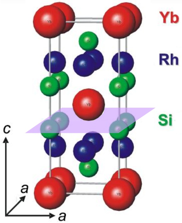
| YbRh2Si2 crystallizes in a tetragonal ThCr2Si2 structure, see figure. Single crystals of excellent quality, i.e. with extremely low density of defects have been grown (average number of defects down to 0.2% of the visible surface atoms, see [87]). So far, six single crystals were cleaved in situ at low temperatures (~20 K) along the crystallographic ab plane. The topography (see below) obtained at 4.6 K evidences an excellent cleave. Here, we employed an Omicron LT STM, again with additional active vibration control. A Fast Fourier Transformation (FFT) of the surface pattern reveals a perfect fourfold symmetry of the surface atoms with distances of 4.0 Å, in excellent agreement with the lattice parameter a = 4.007 Å. | |
| In the following we will concentrate on Si terminated surfaces. The example on the right shows an area of 10 × 10 nm2. The most common defects in the structure of YbRh2Si2 should be an occupation of Si-sites by Rh, occupation of Rh-sites by Si and Si voids. The line scans through the two observed types of defects clearly indicate that these defects cannot be caused by missing or additional atoms. Rather, the most numerous defects observed - the single protrusions - could originate from a larger Rh ion occupying a Si-site at the surface (blue line in the figure on the right). If, however, a smaller Si occupies a Rh-site within the second-to-topmost layer the two adjacent Si in the topmost layer should be affected (yellow line in the figure on the right) resulting in the observed dumb-bell shaped distortion. Here we note that the defect structure as exemplified in this figure has been observed over very large areas and on different samples [87]. Only in one case did we observe a surface of different type (likely Yb-terminated), characterized by individual dents of about 40 pm height change (see Supplemental Information to [81]). It should be emphasized that specifically the line scan perpendicular to the fast scan direction of the STM topography (blue line) underlines the quality of our data with a noise level of about 2 pm. | 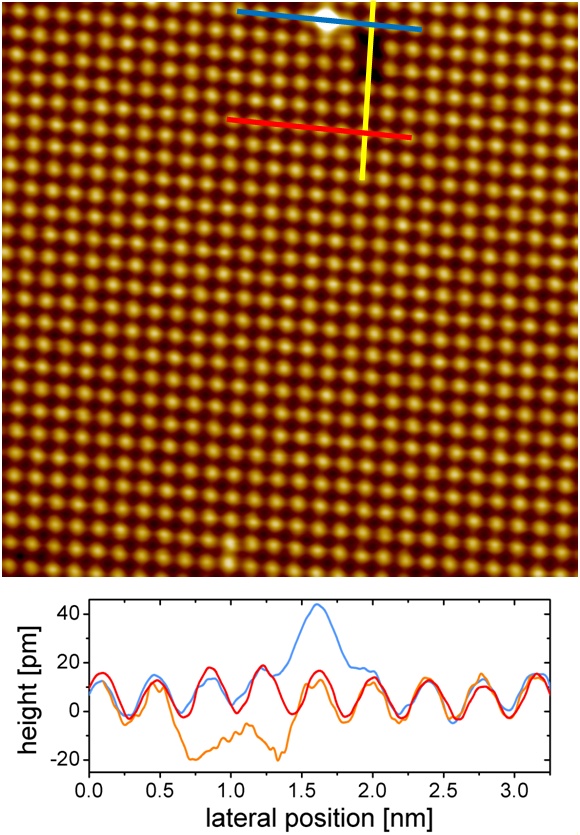 |
| Differential conductances g(V,T) = dI/dV|T obtained by STS on such excellent surfaces at different temperatures are exemplified in the figure to the right. These spectra are dominated by a gap-like feature around zero-bias. At low temperatures, additional peaks can be recognized which can be distinguished by their temperature dependences as discussed below. An analysis of the position in energy of the three peaks marked by the arrows in the figure yields -17 meV, -27 meV and -43 meV. These energies are in excellent agreement with those of the crystalline electric field (CEF) excitations as observed by inelastic neutron scattering (INS, see O. Stockert et al., Physica B 378 (2006) 157). This first (to the best of our knowledge) observation of CEF excitations by STS is of utmost importance as, on the one hand, it indicates that we truly measure bulk properties of our YbRh2Si2 samples and, on the other hand, it supports our conjecture of a Si terminated surface [81]. | 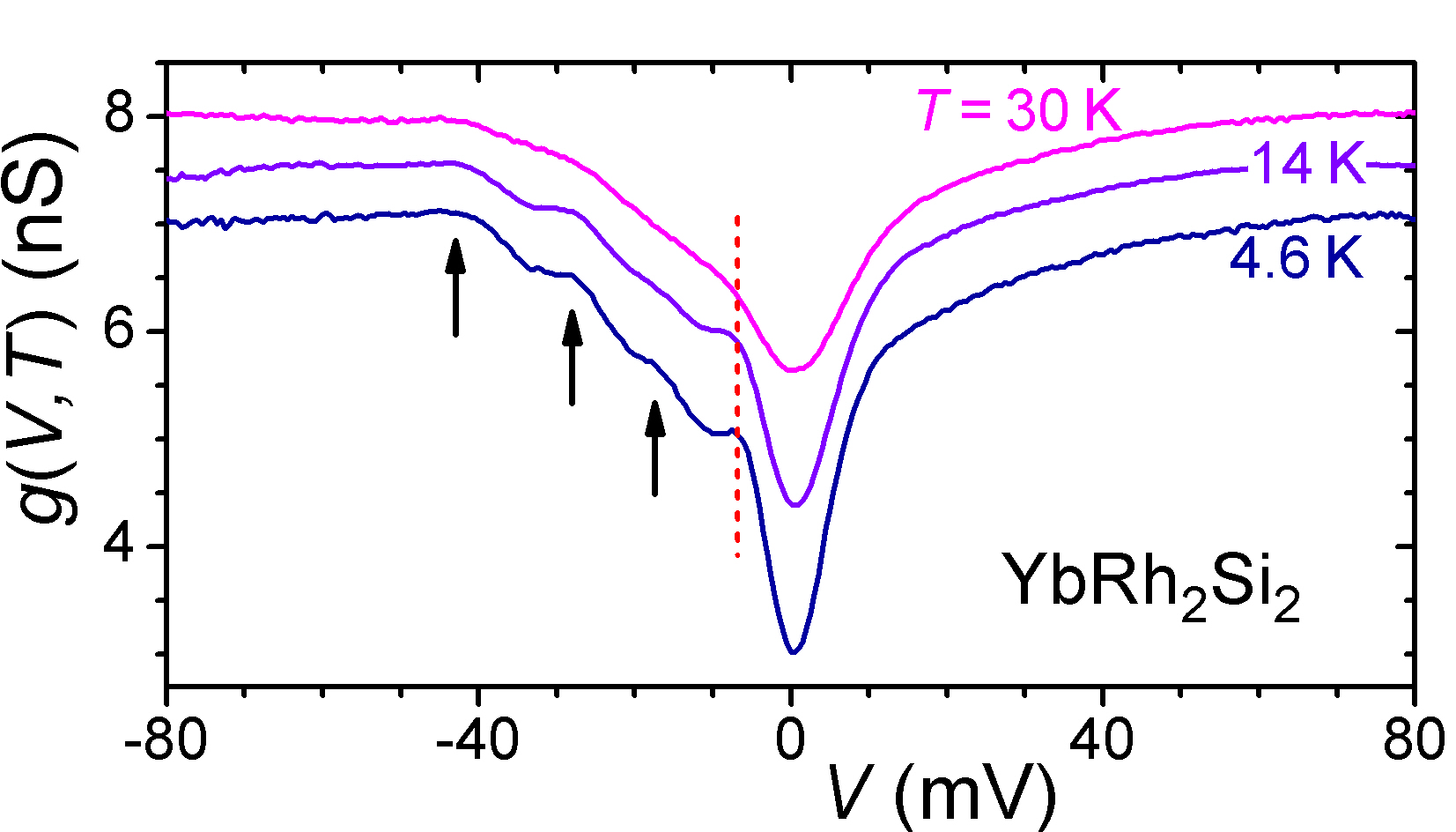 |